The eco-friendly approach could transform the PCB industry by cutting costs, reducing waste, and powering the future of wearable tech.
Researchers at Boise State University have developed a method for manufacturing flexible hybrid circuits that promises to slash production costs, minimize waste, and reduce environmental impact. Their breakthrough, which utilizes laser-induced graphene (LIG), was recently highlighted on the cover of Advanced Materials Technologies.
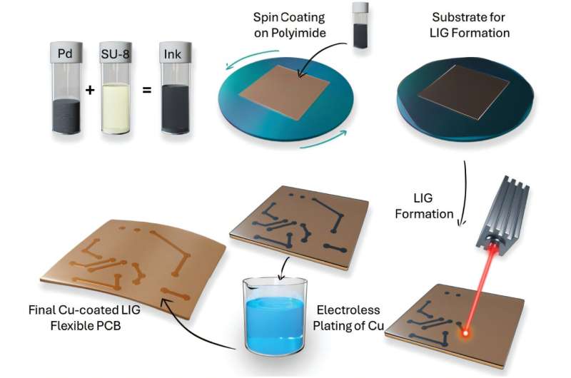
LIG is created through a single-step laser process that transforms carbon-rich materials into a porous, conductive 3D structure, partially composed of atomically thin graphene. This scalable and patternable technique is ideal for next-generation electronics, sensors, and energy storage solutions. The team enhanced LIG by embedding palladium (Pd) nanoparticles into a polymer matrix, enabling the electroless deposition of copper onto the LIG surface. This process forms copper interconnects essential for flexible printed circuit boards (f-PCBs) using a laser-enabled additive manufacturing technique.

These interconnects are integrated with microelectronic components to create a flexible hybrid operational amplifier. The resulting device maintains performance even under repeated bending, demonstrating its suitability for wearable electronics and other flexible sensing applications.“Additive manufacturing of PCBs offers a sustainable path forward for electronics production,” said Attila Rektor, lead author of the study. “Our approach eliminates toxic chemicals and reduces material waste, pushing the boundaries of environmentally responsible manufacturing.”
The global printed circuit board (PCB) market, currently valued at around $90 billion, is projected to exceed $150 billion within the next decade. A key growth driver is the rising demand for flexible PCBs—crucial for lightweight, space-saving, and durable designs in wearable and IoT devices.Professor David Estrada, co-author and faculty at the Micron School of Materials Science and Engineering, praised the recognition: “It’s exciting to see Attila’s work featured so prominently. This research merges scientific innovation with real-world manufacturing benefits—cutting costs while eliminating harmful fabrication steps.”