


This reference design is highly relevant for design engineers working on advanced test and measurement equipment, such as semiconductor testers or high-channel-count instrumentation systems, where achieving precise, low-noise, and scalable signal paths is crucial.
In high-performance data acquisition (DAQ) systems, the analog front-end (AFE) plays a critical role in determining overall signal integrity, resolution, and system accuracy. The reference design provides a practical and optimized solution for engineers aiming to maximize the dynamic range and signal fidelity of their ADC signal chains. It specifically addresses one of the key challenges in AFE design—ensuring full-scale signal swing and low distortion through the ADC driver stage—by implementing a negative supply rail and evaluating both single-ended and differential driver architectures.
The TIDA-01052 reference design by Texas Intsruments (TI) focuses on enhancing and optimizing the analog-to-digital converter (ADC) front-end signal path to support full-scale signal swing propagation through the ADC driver stage without compromising total harmonic distortion (THD). In many data acquisition (DAQ) systems, maintaining high measurement accuracy across the full system dynamic range is essential. To meet this requirement, ADC drivers must accommodate true rail-to-rail input and output signal swings. However, achieving this level of performance is challenging, as most modern operational amplifiers require some headroom from the negative supply to preserve signal integrity.

This design addresses the challenge by introducing an additional negative supply rail. This rail provides the necessary headroom for the ADC driver amplifiers, thereby enabling the signal path to maintain high linearity right down to the system ground. The design evaluates two core ADC driver architectures—single-ended and differential—to offer insights into the trade-offs between simplicity, performance, and noise immunity. By comparing these architectures, the design helps engineers select the best fit for their specific application needs.
Key design theories are outlined to assist engineers in selecting the right components and optimizing their performance. The reference design also includes schematics, PCB layout files, and results from actual hardware testing, making it a complete design package for engineers developing high-performance DAQ modules. The design features two 18-bit SAR ADC channels with support for up to ±5 V input signals. It supports both single-ended and differential input configurations, providing flexibility for a wide range of applications. The front-end is also modular, making it ideal for scalable, high-channel-count systems.

Applications that benefit from this design include automatic test equipment, lab and field instrumentation, and testing systems for semiconductors, LCDs, and memory devices. These applications often involve multi-input systems that require parallel or simultaneous sampling across hundreds or even thousands of channels. Key design goals for such systems include maximizing signal-to-noise ratio (SNR), reducing power consumption, minimizing component count, and controlling cost.
The typical analog front-end (AFE) signal chain consists of multiplexers, programmable gain amplifiers (PGAs), anti-aliasing low-pass filters, and ADC drivers. The ADC digitizes the input signal and outputs it to a host processor such as a microcontroller (MCU) or FPGA. Devices like the OPA827, with low offset and drift, and OPAx625, optimized for low THD and noise, are excellent choices for high-resolution ADC driving. The THS4551 differential amplifier simplifies interfacing from single-ended sources to the differential inputs required by high-precision ADCs.
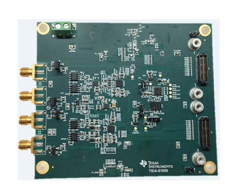
TI has tested this reference design. It comes with a bill of materials (BOM), schematics, assembly drawing, printed circuit board (PCB) layout, and more. The company’s website has additional data about the reference design. To read more about this reference design, click here.