


What if the next leap in electronics lies not in speed or size, but in structure? Mesoporous silicon defies convention—unlocking cleaner, smarter, and more versatile technologies. The future of chips may already be built on pores.
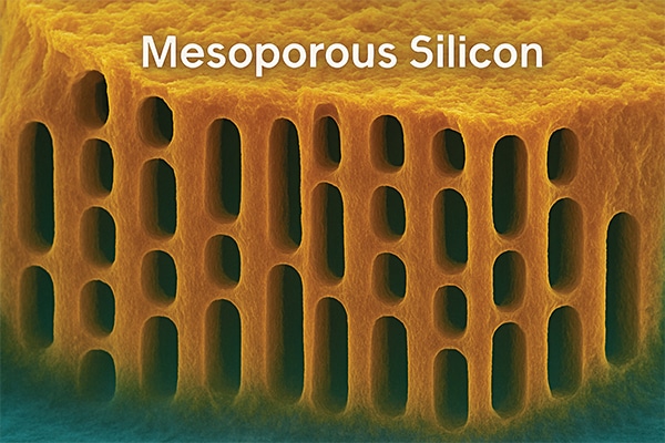
Semiconductors are the backbone of modern electronics, with ongoing advances in materials science continually extending their performance limits. A key breakthrough is mesoporous silicon (m-Si)—a form of silicon featuring a pore network between 2 and 50 nanometres. This distinctive structure imparts exceptional electrical, optical, and chemical properties, making it a strong contender for next-generation semiconductor applications. From high-performance microelectronics to advanced sensing and energy storage, mesoporous silicon is set to reshape the industry.
What is mesoporous silicon?
Mesoporous silicon is derived from crystalline silicon through electrochemical etching, chemical vapour deposition, or other nanofabrication techniques. These processes create a highly porous network that enhances surface area, modifies electronic properties, and enables tunability for a wide range of applications. The pore size and density can be engineered precisely, allowing tailored interaction with light, electricity, and chemicals.
How mesoporous silicon works

Oops! This is an EFY++ article, which means it's our Premium Content. You need to be a Registered User of our website to read its complete content.
Good News: You can register to our website for FREE! CLICK HERE to register now.
Already a registered member? If YES, then simply login to you account below. (TIP: Use 'forgot password' feature and reset and save your new password in your browser, if you forgot the last one!)