


The reference design deliver a compact, high-efficiency solution with reliable power semiconductors and isolation components.
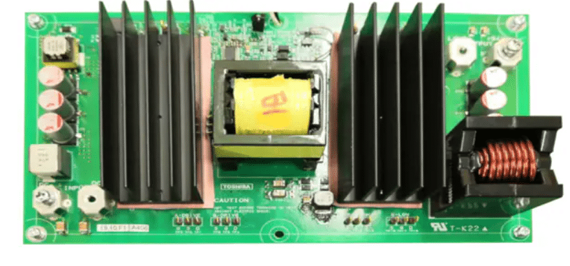
The 1 kW Full-Bridge DC-DC Converter reference design by Toshiba provides a comprehensive solution for high-efficiency power conversion, ideal for use in server power supplies. This design uses a phase-shifted full-bridge topology combined with synchronous rectification to achieve excellent performance in compact form. It is engineered to deliver stable output and high conversion efficiency in demanding server environments where space and thermal management are critical concerns.
The system operates within an input voltage range of DC -36 V to -60 V and provides a regulated output of DC 54 V, delivering up to 1 kW of power. A major highlight of this reference design is its total efficiency of 94.7% under full load conditions (Vin = -54 V), demonstrating its suitability for energy-conscious data center and telecommunications applications. The compact physical dimensions—measuring 207 mm × 120 mm × 45 mm—further underscore its integration potential in space-constrained applications.

At the heart of the power conversion stage are Toshiba’s high-performance power MOSFETs. On the primary side, the design incorporates four TPH2R408QM N-channel MOSFETs. These devices operate at 80 V with an ultra-low on-resistance of 0.00243 Ω at 10 V, leveraging U-MOSⅩ-H process technology and packaged in SOP Advance. On the secondary side, eight TPH1500CNH N-channel MOSFETs are used. These devices are rated at 150 V with an on-resistance of 0.0154 Ω at 10 V, featuring U-MOSⅧ-H technology. Together, these MOSFETs support high-frequency switching and contribute significantly to the converter’s overall efficiency and thermal performance.
To enable precise and isolated communication between the primary and secondary sides, the design includes two TLP2370 high-speed photocouplers. These devices support data transmission rates up to 20 Mbps and provide 3750 Vrms isolation voltage in a compact 5-pin SO6 package, enhancing the reliability and safety of the converter. For output voltage feedback, a TLP291(SE photocoupler is used. This phototransistor-output device ensures accurate voltage regulation and isolation, housed in a 4-pin SO4 package.

The integration of advanced MOSFETs and optoelectronics ensures not only high performance but also ease of design and implementation for engineers developing next-generation server power systems.Toshiba has tested this reference design. It comes with a bill of materials (BOM), schematics, assembly drawing, printed circuit board (PCB) layout, and more. The company’s website has additional data about the reference design. To read more about this reference design, click here.